Integrated Circuit Technology Seminar
This five-day intensive course provides participants with the foundational knowledge of integrated circuit (IC) design and hands-on experience in the fabrication of nMOS integrated circuits. The program is structured to deliver a comprehensive, holistic understanding of the entire field of semiconductor technology.
Integrated Circuit Technology Seminar(in Japanese)
Workshop on Co-Creation and nurturing for Advanced Semiconductor Engineer with a Broad Perspective – CMOS LSI Full Process Course –
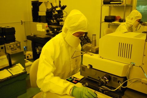
A nine-day practical course focused on manufacturing an image sensor using the Planar CMOS process, which is the fundamental structure of semiconductor integrated circuits.
Participants will gain a thorough understanding of each stage of the CMOS process, including the relationship between planar structure and cross-sectional structure, and will master the overall process flow, along with the physicochemical interrelationships involved throughout all stages.
Practical Training in Integrated Circuit Manufacturing for College of Technology Students (Integrated Green-niX program)
- Basic Course (5 days): Learn the fabrication and design of nMOS integrated circuits, along along with simulation technology.
- Advanced Course (4 days): Focus on constructing and executing the manufacturing process for an integrated circuit that meets a set of given specifications.
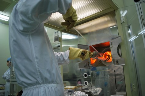
Advanced Practical Training: “Integrated Circuit Full Process” Course (enSET Tokai)
This course mandates that every trainee is assigned a dedicated wafer, upon which they independently perform the comprehensive integrated circuit workflow: process execution, device packaging, and functional evaluation. The goal is to establish a deep comprehension of the full IC process, extending to a command of the correlation between layout geometry (planar) and device profile (cross-sectional), as well as the underlying physicochemical interactions throughout all manufacturing steps.
Basic Seminar and Demonstration of Semiconductor Process Technology
A half-day course providing foundational lectures and practical demonstrations/workshops on semiconductor process technology, customizable based on participant needs.