

MEXT
The Advanced Research Infrastructure
for Materials and Nanotechnology in Japan
Materials Enabling Innovative Energy Conversion
ADVANCED RESEARCH INFRASTRUCTURE for
MATERIALS and NANOTECHNOLOGY in JAPAN
News
No news updates available.
About ARIM JAPAN
To further strengthen Japan’s materials innovation capabilities, the Ministry of Education, Culture, Sports, Science and Technology (MEXT) launched the “Advanced Research Infrastructure for Materials and Nanotechnology in Japan (ARIM)” project in FY2021.
In addition to the shared use of state-of-the-art facilities and support by technical experts, this project collects materials data generated through the use of equipment. Materials data encompasses a wide range of information, including not only material properties but also processing characteristics. The government began providing this data on a nationwide scale in FY2023 to accelerate data-driven research and development.
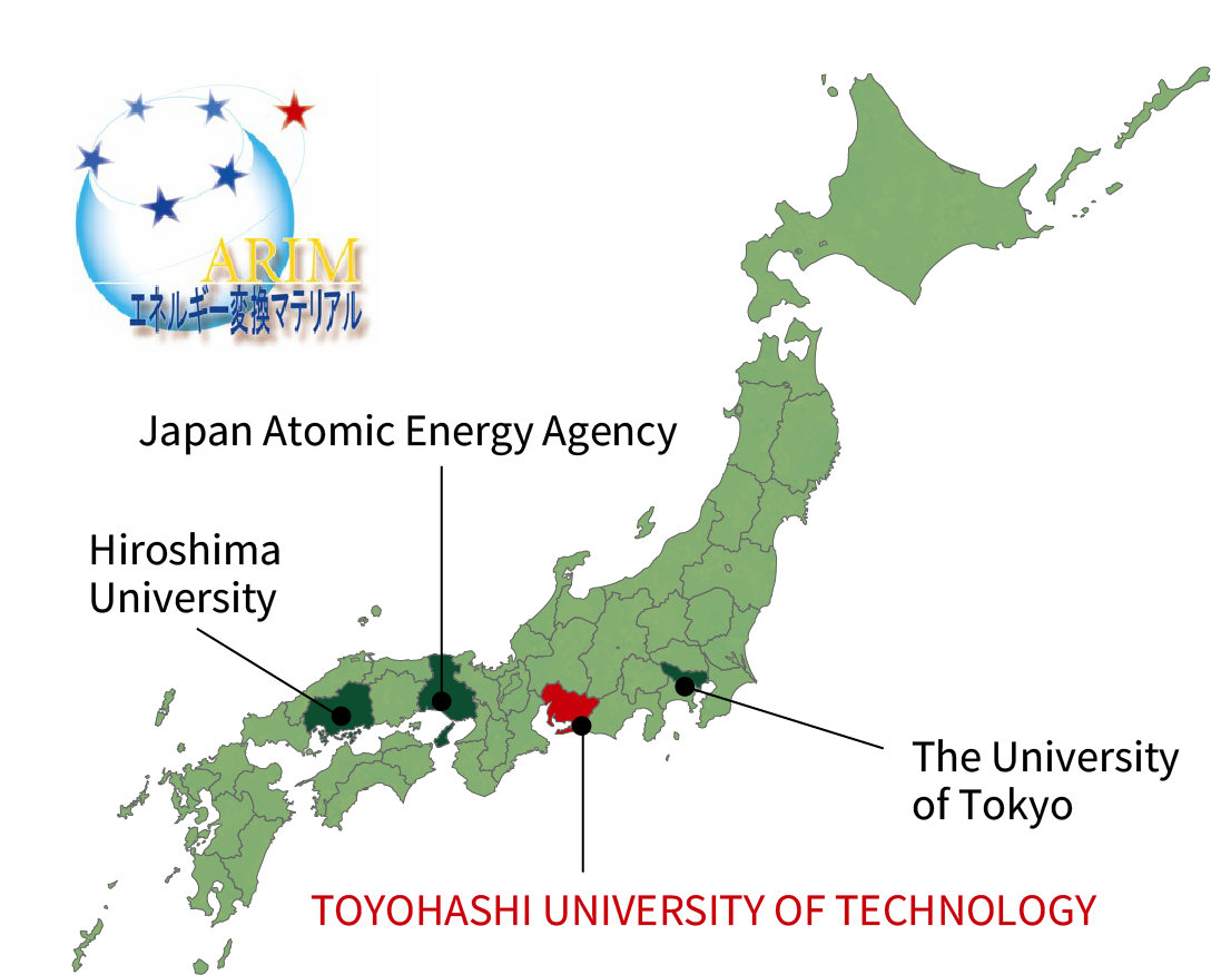
ARIM involves 26 institutions nationwide, establishing a hub-and-spoke system for each of the seven important technology areas. The Center Hub is operated by the National Institute for Materials Science (NIMS). Our university will join the “Materials enabling innovative energy conversion” area (Hub institution: The University of Tokyo; Spoke institutions: Hiroshima University and Japan Atomic Energy Agency) as a spoke institution starting in July 2025. At the same time, we have become a Circuit Prototyping Institute under the ARIM Semiconductor Technology Infrastructure (ARIM-SETI).
through facilities, people, and data
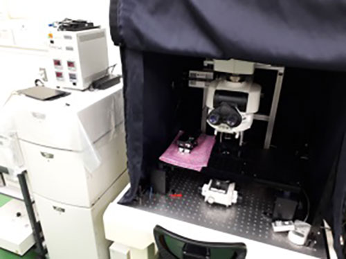
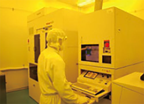
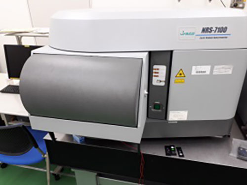
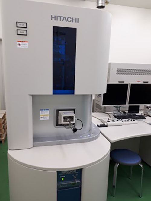
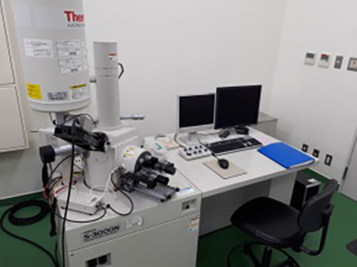
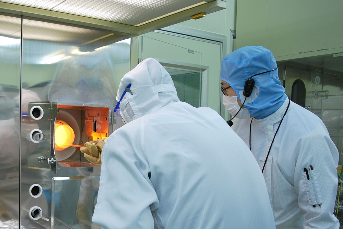
Our university’s Institute of Research for Next Generation Semiconductor and Sensing Science (IRES², known as “Iris”) maintains semiconductor integrated circuit manufacturing and microfabrication facilities compatible with diverse materials, including silicon, compound semiconductors, and various functional materials, to support R&D in next-generation semiconductors and sensors. We are comprehensively equipped with front-end and back-end manufacturing and evaluation equipment covering everything from irregularly shaped materials to 4-inch substrates, providing the fundamental technologies necessary for nano/micro-fabrication and device integration.
Furthermore, in addition to technical staff responsible for equipment operation and research assistance, we have dedicated staff to promote data utilization, supporting device development and evaluation for researchers both within and outside the university, as well as for companies, in diverse ways. Through this, we aim to realize a new form of shared use that includes data, going beyond mere equipment sharing, and to widely return knowledge contributing to semiconductor material and device development to society.